


Overview
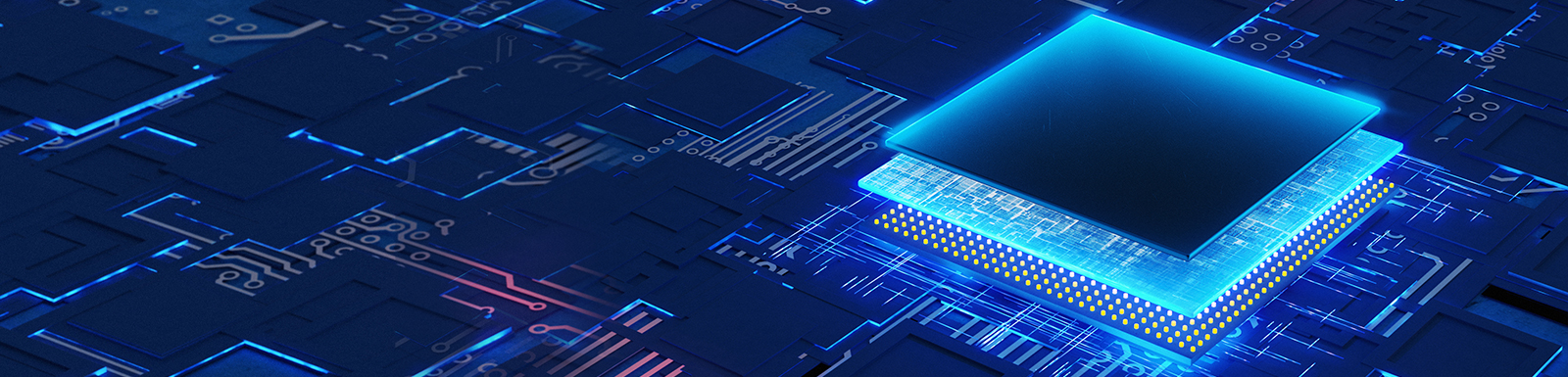
Semiconductors, often in the form of microchips, are crucial components in everything from smartphones and cars to advanced weapons and navigation systems used by the military. Chips must be designed and then subsequently manufactured in facilities known as “fabs,” which can cost billions of dollars and take several years to build. Only a few companies both design and make chips; most specialize in either design or manufacturing. In 2024, Taiwan Semiconductor Manufacturing Company controlled over 60 percent of the world’s contract manufacturing and 90 percent of the manufacturing of advanced chips. With a large percentage of the world’s chip factories located in Taiwan, the global supply chain for chips remains fragile.
KEY DEVELOPMENTS
Moore’s Law, Past and Future For over half a century, a phenomenon known as Moore’s law has governed developments in the semiconductor industry. This refers to a trend in which the number of transistors on a chip of the same size and cost has doubled roughly every couple of years, effectively doubling the chip’s processing power. Moore’s law is not a law of physics but an observed trend driven by improvements in manufacturing tools and other factors that have been so consistent that everyone expects the cost of computing to keep decreasing with time. However, there are indications that Moore’s law has slowed down and that its end may be in sight.
This is happening just as artificial intelligence (AI) and machine learning (ML) are driving a surge in demand for computing resources—especially for specialized hardware such as advanced graphical processing units (GPUs), which power the development and training of many AI and ML models.
Of note: For at least a decade, the name of a chip technology, such as “sevennanometer chip,” has not been an indicator of the size of the chip’s smallest feature. Rather it has been a generational label referring to improved circuit density as the result of extending designs vertically and adopting new materials.
Chiplets and 2.5-D Integration As Moore’s law slows, novel computing advancements are needed. Chiplets are small, modular chips that specialize in specific functions and can be combined in ways that deliver more energyefficient processing power than large, monolithic chips. In 2.5-D integration, an interposer—a specialized substrate—is used to connect chiplets, facilitating faster, more energy-efficient communication. This approach allows high-density memory, high-performance compute units, and communication chips to reside side by side, boosting bandwidth, performance, and power efficiency while reducing the need for full integration on a single chip.
High-Power Density To further improve system performance, compute and memory elements can be moved closer to each other, reducing time delays in sending signals between components. However, closer packing of these elements increases the heat generated per square centimeter. Modern systems generate large amounts of heat: A single GPU generates about a kilowatt of heat and an advanced cluster of them about a megawatt. Traditional air cooling is inadequate, so liquid-based systems are essential.
Memory Technology Developments Innovations like stacking and new materials are advancing memory technology, enabling higher density and performance vital for AI and big data. DRAM and flash have evolved with 3-D structures and complex packaging to support high-bandwidth memory. Magnetoresistive and phase-change memories offer speed and energy benefits.